Computer Nerd Kev |
Home|About|Projects|Links |
Projects > Sig. Trig. > Circuit |
Servo Signal Trigger Circuit Description |
Schematic

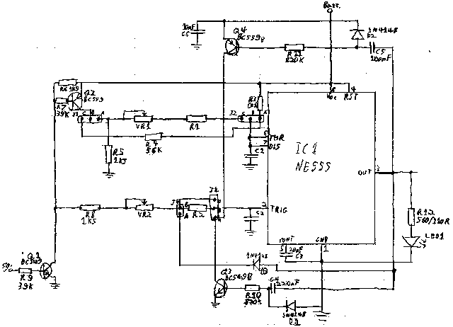
That's my hand drawn attempt at a schematic, note that R12 and LED1 are for testing and an be ignored (unless you want an LED, also the two R12 values are for 12V/6V operation). Click on the image for the full size version (don't worry, it's only 27Kb). Or if you still can't tell it from an ink blot, here's an image of the schematic I did in LTspice.
For the components without values, R3=220K, R1=18K, R2=15K, C1/C2=100nF, VR1/VR2=5K. Check the instructions for different values if using capacitors with different tollerance ratings to those in the kit.
It's interesting to note that this circuit does not use the 555 IC as an oscillator or timer component as it was intended. Particularly in Latching mode, it is instead used for its component parts of two Comparators, a Flip-Flop and a high current output.
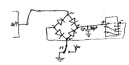
Here's the output circuit for the relay:

Non-Latching
The signal input comes from the receiver and enters Q1 (BC549) through current limiting resistor R9. Q1 pulls C2 to ground through R8, VR2 and R2 and it begins to discharge over a period determined by the combined resistance of these resistors. If this discharge time is shorter than the positive pulse into Q1, the voltage at pin 2 (Trigger) of the 555 timer IC will fall below one third of the supply voltage. This causes pin 3 (Output) of the 555 to go high, powering the Relay through BR1. The diodes inside BR1 prevent the back EMF from the Relay from causing damage to the 555 or preventing it from turning off its power completely.
Once the signal pulse into Q1 goes low, it turns off and C2 charges back to the Supply Voltage in the gap of around 17mS. Also during this time, C1 charges through R3.
Q2 (BC558) is connected to the Collector of Q1 through R7. This PNP transistor therefore turns on with Q1 and charges C1 through R4 (in combination with R3) during a positive signal pulse. This accelerates the charging and causes the Voltage at pin 6 (Threshold) to reach two thirds the supply voltage about 1mS into the positive pulse, which in turn causes pin 3 (Output) to go low. When pin 3 goes low, pin 7 (Discharge) does so also and therefore discharges C1 before the next cycle.
When in the triggered state, pin 6 will therefore turn off the output 1mS before the 2mS positive signal pulse ends. As pin 2 causes the Output to go high at the end of these 2mS, there is a 1mS pulse to ground on the output and this is filtered out after BR1 by C7 to keep the relay from reacting to these pulses. When the trigger button is released, the voltage at pin 2 will not go low enough to cause the output to go high after pin 6 has made it low, therefore the output will go low until a long enough positive pulse is received on the signal input (the button is pressed again).
The purpose of R4 is to minimise the variance in charge time as a result of variation in the value of R3 and C1. R4 acts to reference the input signal pulse in order to synchronize the C1 charge rate with the pulses. It works by increasing the charge rate at the start of the pulse, ensuring it does not take too long to reach two thirds the supply voltage and therefore turning off the Output after pin 2 has just turned it on. R3 is still required to turn off the output if the input pulse is brought to less than 1mS after triggering (which would correspond to an instruction to a servo to turn somewhere between 0° and 90°).
LatchingInstead of C1 charging upon every cycle of the input signal, for Latching mode it is provided with the series resistance of R1 and VR1 to charge through, therefore allowing it to be adjusted to turn off the output via pin 6 (Threshold) only upon a maximum length pulse on the input signal. D3 prevents pin 2 (Trigger) from going low after it has made the Output high and therefore disabling this function (as Trigger over-rides the Threshold pin in its control of the Output).
Q3 (BC549B) and Q4 (BC558B), with their corresponding RC timing networks, form the delay function. This ensures that there is a pause between the Output going On, and going Off in Latching mode, otherwise it would flicker when presented with the trigger signal. The Delay function works by controlling pin 2 (Trigger), as it over-rides pin 6 (Threshold) in control of the Output. A transition of the voltage at pin 3 (Output) from low to high (the output being turned on) causes a positive charge over C4 which discharges to Ground through Q3 via R10, in turn causing pin 2 to be held low which forces the 555 Output to remain high for the discharge time. Q3 works as the inverse of this, as pin 3 (Output) goes from high to low (turns off) C5 is brought to ground and causes Q4 to keep pin 2 high while it charges, preventing the Output from going high. C4 must be twice C5 to compensate for the fact that the pin 2 trigger point, at a third the Supply Voltage, is closer to Ground than the Supply Voltage.
Note that although often considered interchangeable, the BC549 and BC558 transistors used for Q3 and Q4 must be of the "B" hFE classification. That is to say that their full part numbers should be "BC549B" and "BC558B". Use of "A" or "C" types (eg. "BC549C") may cause the delay period to be too short ("A" types), or too long ("C" types). If you are buying transistors for this project, note that some electronics stores that do not state the full part number of the BC5xx transistors they stock may be able to supply specific types upon request.
Non-Latching, Minimum Pulse Length TriggeringThe circuit must be built specifically so as to allow the use of this mode.
For triggering to occur at the minimum pulse length of the input signal, R2 is shorted out and the output is inverted in its action on the Relay. By shorting out R2, the trigger time is determined solely by the series resistance of R8 and VR2, this shorter time means that the triggered state will normally be present unless a minimum pulse length is received. Due to the short pulse length upon triggering, R4 will not be able to ensure that C1 is charged in time, thus it should be replaced with a much lower value resistance, such as the 1K5 resistor not required for R5 by not building the Latching portion of the circuit.
The output of the 555 goes to the Relay through Bridge Rectifier BR1. The purpose of this is to allow selection of either positive or negative triggering depending on whether pin two of BR1 is connected to Supply Voltage or Ground by J5. Additionally, it protects the 555 IC from back EMF from the Relay coil which may harm it, or prevent it from bringing the Output completely to ground. The voltage dropped over the diodes inside BR1 (and the voltage drop of the 555s Output) is compensated for by the use of a 3V Relay.
Transmitter ModificationIn normal operation the transmitter senses the position of the control sticks by monitoring the voltage at the wiper (middle pin) of the potentiometer attached to the control stick assembly. This voltage varies depending on the resistance between positive and ground at either end of the wiper's travel. This forms a voltage divider, thereby presenting to the transmitter a voltage that varies in proportion to the position of the control stick.
By removing the Ground connection from the potentiometer, the voltage is brought to Supply Voltage. This is sensed as position of the control stick at full extent (including trim), and therefore the receiver will be instructed to send the servo (or ESC) a 2mS signal (180° rotation). Similarly, where the Positive connection is removed the voltage at the wiper will go to Ground and therefore instruct the transmitter that the control stick is at minimum extent. The receiver will therefore instruct a servo (or ESC) to rotate 0° with a pulse of around 0.25mS. This is with channel reversal disabled.