USBify V1 R3 Schematic (PDF)
Computer Nerd Kev |
Home|About|Projects|Links |
Projects > USBify > Hardware |
USBify Hardware Description |
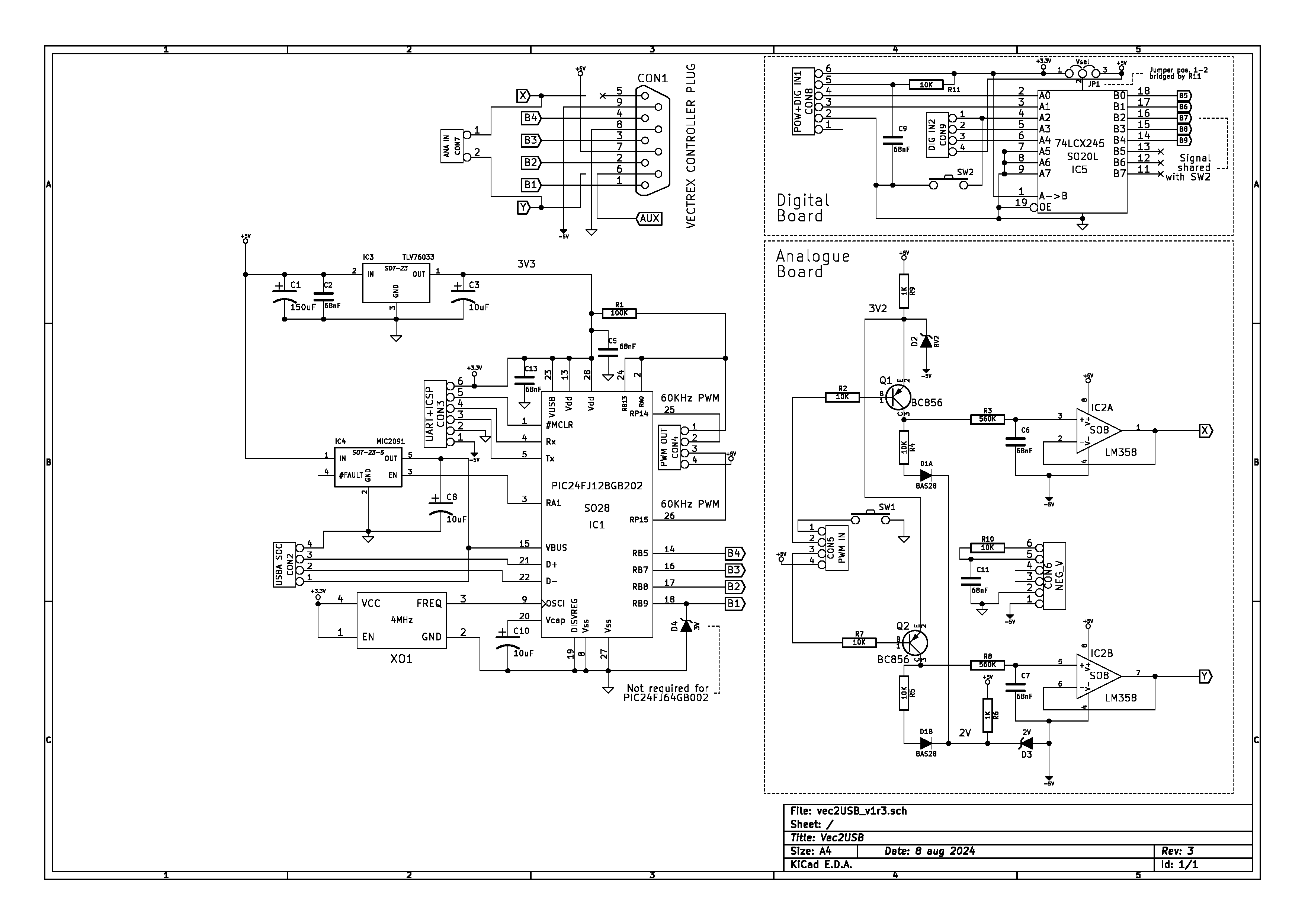
USBify V1 R3 Schematic (PDF)
Usbify uses a PIC24FJ128GB202 (or a PIC24FJ64GB002, with the firmware on a diet) and a PWM DAC circuit for analogue output or a 5V buffer chip for consoles requiring more than four 5V button outputs, mounted on a separate sub-board. One of the sub-board headers (CON3) includes ISCP pins for programming the microcontroller and UART signals for debugging.
The main board, on the left of the schematic page, hosts the microcontroller (IC1). The 5V supply from the console is regulated to 3.3V by a TLV76033 voltage regulator (IC3), and current to the USB port is limited to 100mA by a MIC2091 chip (IC4) that also provides for switching the USB bus on/off with an output from the microcontroller. A 150uF capacitor is fitted on the 5V line as required by the USB 2.0 standard. The 4MHz oscillator module (XO1) is optional - the PIC's internal FRC oscillator can be used instead as its clock source and always seems to work fine with USB devices. 3V zener diode D4 limits voltage over the PIC24FJ128GB202's I/O pin from the 5V controller output B1. The PIC24FJ64GB002 has an extra 5v-tolerant output there, so D4 isn't required with it.
For consoles with analogue inputs, the PIC's PWM module supplies two 60KHz PWM signals corresponding to the joystick position which is filtered by the Analogue Board to produce a corresponding output voltage. The setup button on the sub-board is read from an input that's also shared with a button signal to the Digital Board so that button presses can be detected when the microcontroller output is set HIGH in open-collector mode and the input on pin 2 or 24 is pulled LOW by the button (SW1 or SW2).
The larger header that connects to the sub-boards is also the ICSP header for programming the microcontroller. When a sub-board is attached, it connects the microcontroller's #MCLR input to 3.3V via a resistor (R10 or R11) and a capacitor to GND (C9 or C11) on the sub-board, which enables the microcontroller and avoids accidental resets due to short dips on the 5V supply caused by USB devices. The microcontroller can still be reprogrammed via the ICSP header with a sub-board attached.
For the Vectrex, which has a positive and negative voltage range for its joystick inputs, the 60KHz PWM signals are buffered by PNP transistors Q1 and Q2 which switch voltage levels regulated from the +/-5V supply using zener diodes D2 and D3. Since the zener diodes reference the -5V supply instead of GND, this avoids wobble in the output when connected to controllers like the DualShock 4 which charges up its battery from the USB connection and causes the voltage on the GND and +5V lines to bounce around as the charge circuits turn on and off in a complex pattern. The on time of the transistors switched by the microcontroller's PWM signals determines the charge of capacitors C6 and C7 within a voltage range equivalent to the swing of the potentiometers in the original Vectrex controller. The LM358 dual Op-Amp (IC2) is used in voltage-follower configuration to buffer the voltage level at the capacitors and therefore supply the output signals to the Vectrex. The output of this circuit has a slight offset from 0V at 50% PWM duty cycle which is compensated for in the firmware code.
For video game consoles with more than four 5V digital button inputs, this board provides 3.3V to 5V voltage level conversion for five microcontroller outputs that aren't 5V-tolerant. The B7 output is also sent LOW when the button on the sub-board is pressed because it shares the same signal from/to the microcontroller. A jumper allows selecting whether the buffer chip (IC5) is a normal 5V 74HCT245 type, or an equivalent low-voltage type such as the 74LCX245 chip shown in the schematic.