|
The Logic Visualiser Circuit |

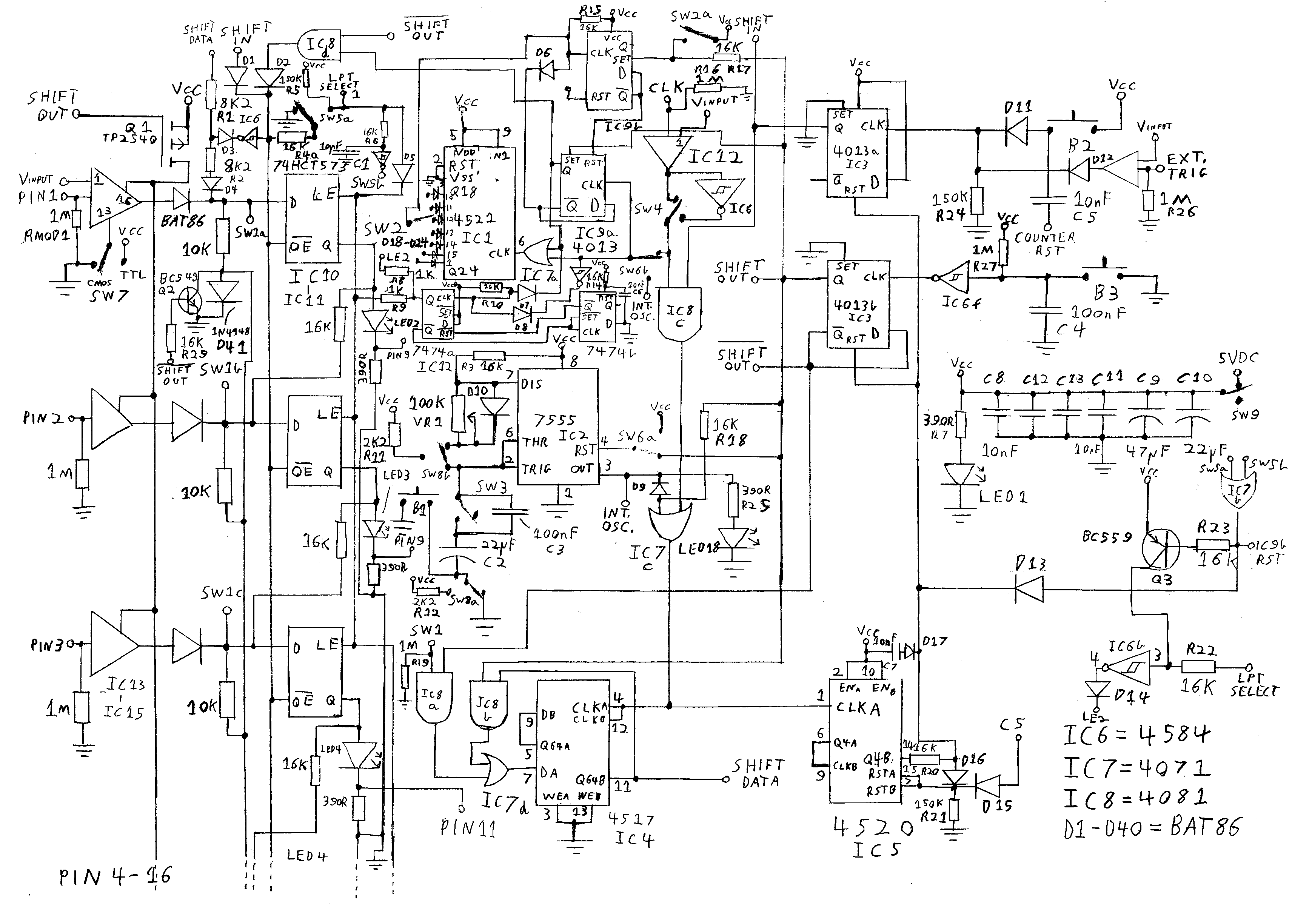
This is the schematic for the Logic Visualiser. The following circuit description is from the "Circuit Overview" section of the Logic Visualiser booket. A more detailed examination can be found further in Chapter III of the booklet, which may be downloaded from the main Logic Visualiser web page.
Only the first three input stages are shown in the schematic, with the others following the same pattern. The LE and #OE inputs of each IC10-IC11 latch are connected together internally, and are not connected between the two ICs. Note that D1, D2 and R4 are duplicated for the #OE input to IC11. These are shown on the PCB as D1a/b, D2a/b and R4a/b. R4b connects with SW5b, while the diodes connect with the same signals as their "a grade" counterparts.
Circuit Overview
At intervals determined by the circuitry associated with the active operating mode, the IC10-IC11 (74HCT573) 8bit Latching Bus Buffers alternate between sampling input data and displaying it on the sixteen output LEDs. In the Internal Oscillator and Pulse operating modes this sampling occurs at an interval determined by the user, whose wishes are converted into electronic commands by IC2 (ICM7555), a CMOS version of that ever popular NE555 timer IC which does so love to pop up in circuits like this.
A slightly more involved sequence of interactions is required for the Clock Division mode which must ensure that the input is sampled one clock period after the relative position where it was sampled previously, and at slow enough intervals that the human operator is still kept in on the fun. The IC1 (4521) 24 Stage Counter IC with its seven output taps provides a suitable delay between updates. Meanwhile dual flip/flop IC9 (4013) triggers the input latches at the end of a cycle, while simultaneously preventing IC1 from seeing the following clock pulse, so that its count will inadvertently "gain" one ahead of its last cycle.
In External Output mode, the timing signals are left entirely to the judgment of whatever computer, or other device, chooses to talk on the LPT SELECT input. Whether this input is High or Low determines whether the first or second bank of eight latches (IC10-IC11) is showing its latched data on the data outputs.
Things are a little different for Data Sampling mode. For data input, all the data latch outputs are disabled and the input is taken straight from the input buffer selected by SW1. A signal on the External Trigger input, or a user pressing the Sample Data button, causes the data to be shifted into IC4 (4517) Dual 64bit Shift Register while IC5 (4520) Dual 4bit Binary Counter waits until it's full. IC3 (4013) Dual Flip/Flop starts this sequence when the B2 push button or External Trigger input is asserted, and when the IC5 counter reaches 128, it is reset and the device gets back to what it was doing before.
Data display operates similarly, except that now the IC13-IC15 (4504) input buffers are disabled instead of the latches, and the latch outputs are constantly enabled so that IC10-IC11 acts as one big parallel output shift register. Data is fed into this from IC4, while the same data is fed back to its own input so that it can be viewed again later. Again, the IC5 counter stops the sequence when the end of the stored data is reached by resetting IC3 which began the display by latching the input from B3.
In the optional Alternative External Output mode, the input latches are configured in "transparent" mode, where they act simply as further data buffers. Alternate inputs to IC10-IC11 must be pulled low to prevent data "flowing through" between inputs and outputs as in Data Sampling mode during display.
Content Copyright Kevin Koster 2018