LCD Shutterglasses
Rainbow Adapter
Usage
Construction
Circuit Description
For the official kit from
OmberTech
By Kevin Koster
2018
Contents
|
Introduction
|
|
|
|
Usage
|
|
|
|
Construction
|
|
|
|
Parts List
|
|
|
|
Resistors and Diodes
|
|
|
|
Integrated Circuits
|
|
|
|
MKT Capacitors
|
|
|
|
Electrolytic Capacitors and
LED
|
|
|
|
Switches
|
|
|
|
Wires
|
|
|
|
Enclosure Assembly
|
|
|
|
Modifying Wireless
Shutterglasses
|
|
|
|
Theory
|
|
|
|
LCD Elements
|
|
|
|
Circuit Description
|
|
|
The rainbow adapter for LCD
shutterglasses uniquely exploits a refractive effect exhibited in liquid
crystal display "elements" when fading out from their opaque
state. This allows a rainbow of colours to be viewed surrounding reflective
objects.
The following page describes usage of
the adapter, then we move on to a step-by-step description of how to
construct the adapter kit, as well as modify an unwanted pair of active 3D
shutterglasses for use with it. Then finally, we look at exactly what
electronics are required in order to put rainbows in your eyes.
With four AA batteries fitting snugly
in the battery holder, a simple flick of the "Power" switch while
the "Boost" switch remains off will begin powering the
shutterglasses with the alternating drive signal that produces the
refractive "rainbow" effect. Within thirty seconds a halo of
multicoloured bands should be visible around lights, windows, and white or
reflective objects. After about a minute, the effect should have built up
fully.
The effect is most visible in more
dimly lit areas out of direct sunlight, or outdoors at sunrise or sunset.
Hold a piece of white paper in the sunlight shining through a window to see
rainbow coloured images of it "floating" above on either side.
When outdoors, face away from the sun to view the reflected light to best
effect, remember never to look directly at the sun.
When Boost mode is enabled, the drive
voltage to the shutterglasses is increased and the effect is made brighter
and more vivid. However this may cause instability in the circuit, and in
any case the effect will fade and become less defined shortly after this
mode is enabled. Turning Boost mode off again returns to regular
performance.
Some faint flickering will be visible
while the glasses rapidly fade in and out. Take a break if this begins to
cause headaches or nausea.
The adapter can connect to most wired
3D shutterglasses designed for use with PC 3D graphics adapters or TVs
when they are equipped with a 3.5mm stereo plug. Some models may produce
the effect while some may not, the only way to know is to give them a try.
Wireless adapters require modification
to connect wires from the adapter circuit directly to the LCD "lens"
elements. This is described in the following section.
If you have purchased the rainbow
adapter kit from OmberTech, you are likely reading this in the company of
an assorted bag of bits (described more exactly in Figure 1) that you hope
to turn into the driver for your new rainbow tinted glasses. This chapter
will guide you though step-by-step in the fulfillment of this goal. So grab
your soldering iron and let's get started!
This kit doesn't use any CMOS devices,
so no special static precautions are required when handling the components.
|
Part
|
QTY
|
Identifiers
|
Marking
|
|
100nF MKT Cap.
|
3
|
C1, C2, C3
|
104J100
|
|
4.7uF Electrolytic Cap.
|
1
|
C4
|
4.7uF
|
|
22uF Electrolytic Cap.
|
1
|
C5
|
22uF
|
|
1N4148 Silicon Diode
|
2
|
D1, D2
|
1N4148
|
|
4.7V Zener Diode
|
1
|
ZD1
|
TZX 4V7 C
|
|
3mm LED
|
1
|
LED1
|
|
|
74LS74 Flip-Flop IC
|
1
|
IC1
|
SN74LS74AN
|
|
74LS126 3-State Buffer IC
|
1
|
IC2
|
SN74LS126AN
|
|
555 Timer IC
|
1
|
IC3
|
SE555P
|
|
47ohm Resistor
|
1
|
R7
|
Yel, Ppl, Blk
|
|
1.2Kohm Resistor
|
1
|
R3
|
Brn, Red, Red
|
|
2.2Kohm Resistor
|
2
|
R4, R5
|
Red, Red, Blk, Brn (Green body)
|
|
3.3Kohm Resistor
|
1
|
R6
|
Ong, Ong, Red
|
|
56Kohm Resistor
|
1
|
R2
|
Grn, Blu, Blk, Red, Brn (Green body)
|
|
100Kohm Resistor
|
1
|
R1
|
Brn, Blk, Yel
|
|
DPDT PCB-Mount Switch
|
2
|
SW1, SW2
|
|
|
|
|
|
|
|
3-Way Ribbon Cable
|
1
|
|
|
|
4xAA Battery Holder
|
1
|
|
|
|
50x50mm Circuit Board
|
1
|
|
V. 1, PCB R. 1.0
|
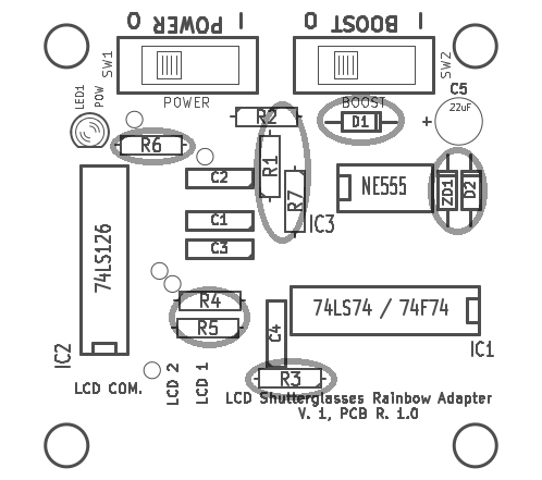
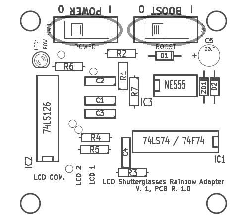
We begin with the resistors and diodes.
Resistor values are shown in Table 2 below. Ensure that the black band at
the end of the diodes matches the corresponding mark on the silkscreen
image.
|
Identifier
|
Value
|
Marking
|
|
R1
|
100K
|
Brn, Blk, Yel
|
|
R2
|
56K
|
Grn, Blu, Blk, Red, Brn (Green body)
|
|
R3
|
1K2
|
Brn, Red, Red
|
|
R4, R5
|
2K2
|
Red, Red, Blk, Brn (Green body)
|
|
R6
|
3K3
|
Ong, Ong, Red
|
|
R7
|
47R
|
Yel, Ppl, Blk
|
Table 2,
Resistor Values.
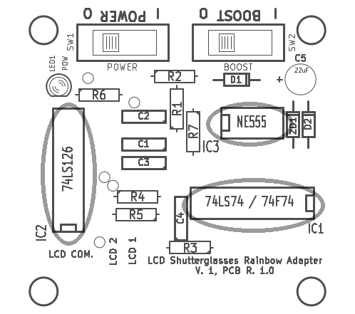
The ICs are now soldered into place,
watching that the notch or round mark on the their top matches the mark on
the silkscreen image.
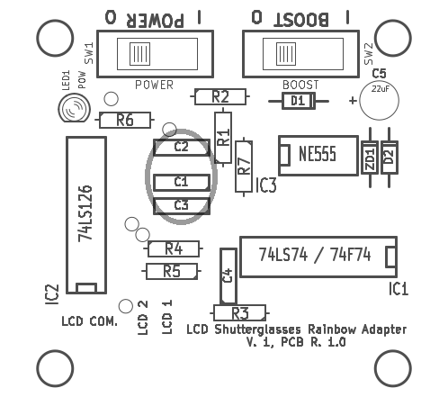
These little grey blocks of capacitance
are all lined up in the middle of the board, time to plop them on.
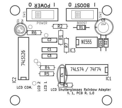
The remaining capacitors and the power
LED now get their turn. There's no mark indicating the orientation of C4 on
the silkscreen, but it should be orientated with the negative side (marked
by the stripe and the shorter lead) closest to the center of the board. C5
is orientated with negative facing outwards from the board, as indicated by
the little "+" symbol on the silkscreen. Also watch that the
notch on the body of the LED (and the shorter lead) match the image on the
silkscreen.
C4 can be bent down over R4 and R5
before soldering, and the same done to C5 on top of ZD1 and D2. If using
the optional second board mounted above for protection, bend the LED
sideways as well so that it sticks out the side and is visible when
everything is assembled.
The only components missing from the
board should now be the switches. Try to get the "legs" of the
switches resting flat against the board so that minimal stress is put on
the connections during use, and also to make sure that they don't end up
too high if you're using the optional second board for protection.
Wire connections are brought in from
the top of the board and fed through holes in order to prevent strain from
twisting at the solder joints. The grey three-way ribbon cable for
connecting with the glasses is parted and the individual wires can be
pulled through the holes with their insulation using pliers. The Power
wires from the battery holder turned out to be a little thick for this, so
only the core wires may fit through the holes, stripped of their insulation.
Once through to the solder side of the
board, the wires are soldered to the long pads described by writing on the
silkscreen or copper layer. The "LCD COM." pad is broken into
two, and the wire must be soldered over both of these pads.
If you're using wired glasses with the
adapter, you can solder a 3.5mm socket onto the end of the ribbon cable to
connect with the plug from the glasses. Make sure to connect the "LCD
COM." wire with the base of the 3.5mm plug, and the LCD 1/2 wires to
either the middle or the tip with no preference to which.
Final Checks:
With the circuit board completed, now
is the time to check over your work for any of those pesky components that
like to hop into the wrong position, or spin themselves the wrong way
round, while you're not looking. While you're there, check the bottom of
the board for any missed or bridged solder joints.
If you're happy with the board on its
own, or you have your own case, you can now start using your wired glasses
with the rainbow adapter, or move over to the section on modifying wireless
glasses to connect them to it.
If you bought the optional second board
to mount above the adapter circuitry for protection, now you can install it
using the nuts, bolts, and plastic spacers supplied.
The outer screw holes in the battery
holder are aligned with the holes at the switch end of the adapter board,
and the bolts run through from the battery compartment side. Drop the
spacers onto the bolts and do the same with the bolts at the other end
before installing the second board with the notched end above the switches
to allow easy access. Add the nuts to the end of the bolts and tighten the
bolts with a flat head screwdriver while gripping the nuts with pliers.
Additional protection might be achieved by wrapping the sides in electrical
tape, while making sure to leave the power LED visible.
Results with different models of
shutterglasses have been mixed. While the old PC wired glasses optionally
offered for sale with the adapters, and a pair of HiSense brand wireless
glasses for 3D TVs from 2011 have worked, a pair of SamSung 3D TV glasses
from 2013 failed to work with the adapter. Although these latter glasses
briefly showed the effect while unplugging them from the circuit, no timing
arrangement in the circuit has succeeded in making it visible for any
length of time. In the end it just comes down to "try it and see".
To attempt such a try, the first step
is to break into the circuitry that controls the LCD "lenses" and
cut the connections before wiring them directly to the adapter. The
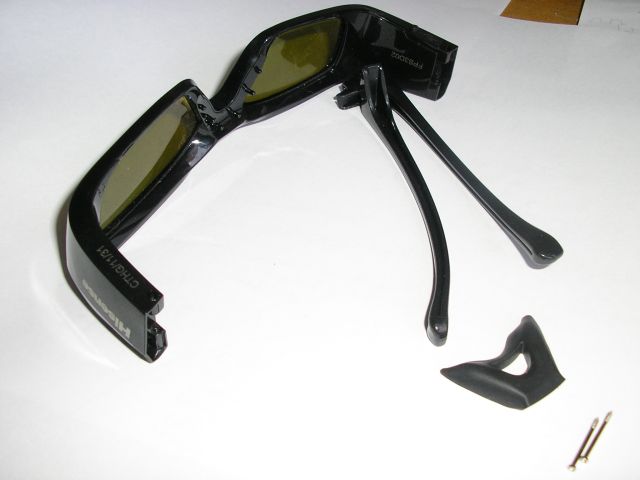
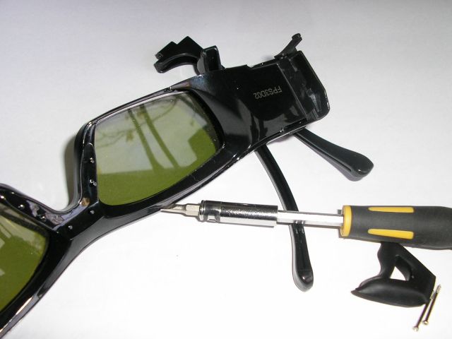
following pictures show disassembling the Hisense brand glasses, model
FPS3D02.
First remove any screws that are
present. Look around the hinges.
Next the plastic clips that hold the
glasses together will have to be prised apart. Use a flat head screwdriver
to slip into the gap and lever the front apart from the back. The strength
of the clips can vary and it may be impossible to separate the halves
without damaging the plastic, but try hard to avoid putting pressure on the
glass it can easily crack. The middle is the most difficult part.
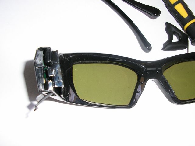
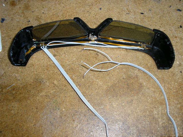
Once inside, the lenses on modern
glasses seem often to be connected using a flexible PCB. On the SamSung
glasses it was easy to solder the wires onto the solder pads connecting the
lenses to the flex, then the control board was cut off to prevent it
interfering. On the HiSense glasses, the wires had to be carefully soldered
to the contacts at the end of the flex where it was meant to fit into a
connector on the control board.
SamSung Glasses
Hisense Glasses
Remember that the LCD 1/2 wires can be
interchanged, but the LCD COM. wire must be the one that connects to both
of the lenses. Polarity is not important.
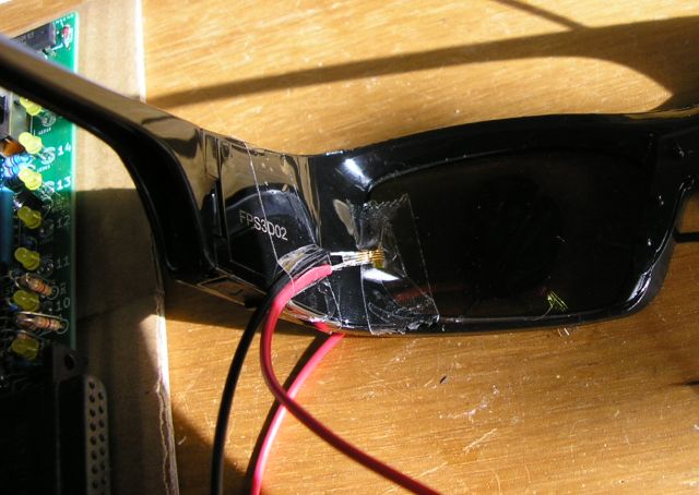
Once all the wiring is done, the case
can be pressed back as well as is possible (it may need to be glued if the
wire pushes the halves too far apart, or the clips have all broken). Then
the screws are put back, and with a bit of luck you can put the glasses on
and let them bring some brand new colour into your world.
The "lenses" in the LCD
Shutterglasses are equivalent to single pixels in a monochrome Liquid
Crystal Display, or single elements of a 7-segment numeric display. The "D"
in "LCD Shutterglasses" is therefore out of place because there
is nothing that can really be displayed by glasses with lenses that in
normal use can only be transparent or opaque.
From an electrical perspective the
elements themselves act as capacitors. When charged, the Liquid Crystal
molecules align to straighten out a twist in their structure that otherwise
rotates the polarisation of light passing through. By placing polarising
filters either side of the crystals, when the polarisation of the light is
opposite to the outer filter, no light can get through at all. Depending on
the filter this can happen in either the charged or discharged state of the
LCD element. Most commonly it is in the charged state, so when a signal is
applied the element becomes opaque.
It would seem that this signal might
simply be a fixed voltage difference, but to complicate matters LCD
elements perform best and live longest when the polarity of their charge is
constantly changed. The signal therefore needs to be rapidly alternating
from High to Low in opposite states across the LCD element's two electrical
connections. Then it appears opaque until the element is shorted so that it
can allow light to pass through once more.
In this circuit we add one more input
state for this capacitive LCD element, which discharges it slowly so that
it fades out rather than being shorted out and made immediately
transparent. A possible explanation for the resulting effect is that the
slow discharge results in the liquid crystal molecules lingering in a
partially twisted state, thereby partially rotating the polarisation of the
light traveling through. The wavelength of the light influences the degree
of rotation that takes place, so the different colours of light become
visible in bands, as in a rainbow.
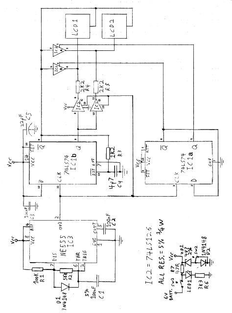
Figure 1, Schematic.
IC3 is that old favourite the 555
timer, here configured with D1 ensuring a longer On time than Off time by
allowing C1 to bypass R2 when it charges while the output is High.
At the same time as this output is
High, IC2c/d (74LS126) are enabled, allowing the non-inverted output of the
IC1b (74LS74) Flip-Flop to be applied to R4 and R5. When the clock signal
from IC3 goes from Low to High, the Flip-Flop output likewise goes Low to
High as well. But at the same time C4 begins to discharge via R3, connected
to the Flip-Flop's inverted output, and eventually causes it to reset,
bringing the non-inverted output back Low again.
This oscillation alternately charges
the active LCD element because the opposite states of the inverted and
non-inverted Flip-Flop outputs are applied to it.
Meanwhile, the inactive element is
shorted out by either IC2a or IC2b. These force both of the LCD connections
to an equal voltage and thereby discharge its capacitance. The active
element is alternated on each clock cycle by Flip-Flop IC1a which toggles
the Enable inputs of the IC2a/b 3-state buffers.
The connection of the Enable inputs of
the other 3-State buffers IC2c/d to the clock signal allows the active LCD
element to be discharged slowly for the Low period of the clock waveform
(set by R2) when all the buffers on one of its connections are in 3-State
mode. This fades out from the charged, opaque, state that it was in during
the preceeding High period of the clock waveform. The complete resulting
output waveform is shown in Figure 2.
Finally, the effect was found only to
work at drive lower voltages to the LCD elements, but with an increased
brilliance when the circuit supply voltage was quickly raised from around
4.75V to above 5V, before fading out. The power regulation part of the
circuit, shown in the bottom left of the schematic, makes sure that the
normal supply voltage is set for optimal performance by using ZD1 to keep
it within 2% of 4.7V. SW2 effectively switches a silicon diode in series
with ZD1's path to GND, increasing the voltage across it, and therefore the
circuit supply voltage, by at most about 0.7V. This provides the "Boost"
functionality, but unfortunately also introduced circuit instability with
some 74LS74 ICs. The power LED is connected to the unregulated part of the
supply to prevent unneeded power dissipation across R7.
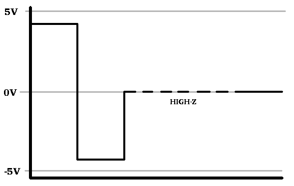
Figure 2,
Output Waveform. Shows voltage measured over LCD
COM. and either LCD 1 or LCD 2 output, with no LCD element connected.
Begins at the rising edge of the clock cycle. The dotted line indicates
that both output buffers on the LCD output are in 3-State mode.