


PiTrex_Discrete
- Edit
- Recent Changes
- Advanced Search
- All Pages
- Administration
- Index
PiTrex_Discrete 
This page describes technical details of the PiTrex Discrete interface cartridge designed by Kevin Koster. See the Hardware_Description for general information.
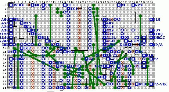
Schematic

PiTrex Discrete Schematic

Schematic CAD Version
CAD Schematic PDF

Cartridge Connector Pinout PDF
Raspberry Pi GPIO Pin Assignments
The Raspberry Pi GPIO is read and written as one 32bit byte. The pin assignments for the Data and Address bus are therefore arranged with respect to the order of bits in the GPIO register, so that the separate Data and Address bytes can be shifted into position using the "<<" shift-left operator, and all written with a single GPIO register write operation.
| Description | Bit | Pin | Note |
| D0 | 16 | 36 | |
| D1 | 17 | 11 | |
| D2 | 18 | 12 | |
| D3 | 19 | 35 | |
| D4 | 20 | 38 | |
| D5 | 21 | 40 | |
| D6 | 22 | 15 | |
| D7 | 23 | 16 | |
| A0 | 7 | 26 | |
| A1 | 8 | 24 | |
| A2 | 9 | 21 | |
| A3 | 10 | 19 | |
| A12 | 11 | 23 | |
| A14/A15 | 12 | 32 | |
| R/#W | 13 | 33 | |
| PB6 | 5 | 29 | |
| IRQ_LATCH | 6 | 31 | |
| RDY(#OE) | 24 | 18 | |
| LATCH_EN | 25 | 22 | |
| IRQ | 26 | 37 | |
| #HALT | 27 | 13 | Jumper to GND on Pi0 |
| #D/A | N/A | 9 | GND on Pi0 |
| 3V3 | N/A | 1 | |
| 5V | N/A | 2 | |
| GND | N/A | 6 |
Unused GPIO Pins
| Bit | Pin | Alt. Function | Note |
| 0 | 27 | ID_SD | The Raspberry Pi Zero Schematic Notes that this pin should only be used for EEPROMs used for Pi HAT boards |
| 1 | 28 | ID_SC | The Raspberry Pi Zero Schematic Notes that this pin should only be used for EEPROMs used for Pi HAT boards |
| 2 | 3 | I2C1 SDA | I2C Bus |
| 3 | 5 | I2C1 SCL | I2C Bus |
| 4 | 7 | GCLK0 | General-Purpose Clock |
| 14 | 8 | UART TXD | UART |
| 15 | 10 | RXD | UART |
| 28 | None | PCM_CLK | Not exposed on GPIO Header. Probably used with audio DAC on other Raspberry Pi boards |
| 29 | None | PCM_FS | Not exposed on GPIO Header. Probably used with audio DAC on other Raspberry Pi boards |
The UART on pins 8 and 10 can be used for connection to the Linux serial console. Note that the ALT function setting is different between the Raspberry Pi Zero and Raspberry Pi Zero W. For the Raspberry Pi Zero, Linux will use the serial port (UART0) on ALT0 by default. For the Raspberry Pi Zero W, ALT5 (UART1 (Mini UART)). This must be remembered when writing to the GPFSEL1 register to set the function of other pins.
Pins used for PWM sound were not left free, though interest in using these for a simple sound output on a later PiTrex version has been voiced. PWM0 can be assigned to either GPIO bit 18 (pin 12, used for D2 on PiTrex) or GPIO bit 12 (pin 32, Pitrex A14). PWM1 can be GPIO bit 19 (pin 35, PiTrex D3) or GPIO bit 13 (pin 33, PiTrex R/#W). R/#W would probably be easiest to move out of the way, maybe to GPIO bit 4 (pin 7, unused).
Circuit Description
Two flip-flops (IC3, 74HCT74) are clocked from the #E signal which is an inverted version of the interal 1.5MHz clock signal used within the Vectrex, exposed at the Vectrex cartridge port. These control the #OE inputs of the 74LVC646 latching bus buffers, allowing the Address and Data bus outputs to be activated for every other cycle of the Vectrex clock. When not active, these outputs are in a high-impedance state. This action is disabled (assuming that the IRQ LATCH function described below is not used) when the LATCH EN input from the Raspberry Pi is Low. In order to prevent the outputs from being disabled before then end of an #E clock cycle, the Q output of IC3a, which is High when #OE is enabled on the bus buffers, is fed back to the #RST inputs of the flip-flops via D2 and R3, so that operation is only disabled after the active cycle is ended.
The buffers sample the state of their inputs when their clock input transitions Low-to-High. The flip-flop IC3a and AND gate IC4a (74HCT08) ensure that this corresponds to the correct point of the Vectrex's clock signal to interface with the VIA. In write mode, both buffers read data from the Pi with their "B" I/O pins and write to the Vectrex on their "A" I/O pins. Correspondingly, the "CLK B-A" inputs control when the Data bus is sampled. In Read mode, IC2 needs data to flow from the Vectrex to the Pi, so the "CLK A-B" input is used and this is configured so that the data bus from the Vectrex is sampled on the cycle following the output of the Address to the VIA.
Two 74LVC646 latching bus buffers are used. IC1 controls the Vectrex Address bus lines that are required for interfacing with the 6522 VIA chip. Only A0 through A3 are the actual Address selection lines for the VIA. A12 connects to its Chip Select 1 input (CS1), while A14 and A15 are combined by a NAND gate inside the Vectrex to control the #ROMS signal as part of the Vectrex's discrete address decoding logic, which enables Chip Select 2 (CS2) on the VIA. One buffer output supplies both A14 and A15 because with there is no need to control them independently.
When the buffer is set in the high-impedance state, pull-down resistors R13-R18 ensure that VIA communication is disabled. Address inputs not used for communication with the VIA at all are permanently tied Low via resistors R19-R27, a lower resistance being required for R26 and R27 because these must supply current for TTL inputs rather than lower-power CMOS inputs.
The R/#W signal from the Pi also passes through IC1 to control the corresponding input to the VIA. Additionally, it determines the direction of signals passing through the second 74LVC646 buffer, IC2 (using its DIR input), which connects with the Vectrex's data bus. In Read mode, the data outputs to the Pi are active for the whole duration that LATCH EN is High. So Q1 (an inverter constructed from a single NPN transistor) asserts the #SET input of IC3b in Read mode so that the #Q output is Low, asserting IC2's #OE input, so long as #RST is not asserted due to LATCH EN going LOW (while IC3a's Q output is LOW) because this overrides #SET and forces IC3b's #Q output HIGH. The flip-flop may be set to an invalid state if both R/#W and LATCH EN are set at the same time by the Pi, however this would in any case not respect the set-up time for the buffers and potentially result in the R/#W input being misread by IC1. The LATCH EN signal should always be set with a separate write operation to the Pi's GPIO following the setting of the Data and Address signals.
Voltage Levels
The Pi's GPIO uses 3.3V CMOS logic levels, whereas the Vectrex uses 5V TTL levels. At 3.3V, CMOS levels (approximately under 1.1V = LOW, over 2.2V = HIGH) are almost compatible with the voltage thresholds of TTL inputs (approximately under 0.7V = LOW, over 2.4V = HIGH). As such, 5V TTL compatible HCT CMOS logic chips are used for the AND gates (74HCT08) as well as the flip-flops (74HCT74), their inputs able to read signals from both the Vectrex and the Pi (from which the HIGH signals are not so heavily loaded as to risk dropping below 2.4V). For the #OE output from flip-flop IC3a to connect with the Pi's GPIO, which could be damaged by 5v TTL HIGH levels, D1 ensures that the signal only pulls LOW the input connected via R1 to 3.3V. To ensure that the voltage drop over this diode added to the maximum LOW level voltage from IC3a does not exceed the GPIO input's LOW threshold, a Schottky type diode with low forward voltage drop (at this current) is used.
The 74LVC646 bus buffers are designed for interfacing 3.3V CMOS with 5V TTL systems. Unlike the PiTrex's other logic ICs, these are powered from the Pi's 3.3V supply, and as such they are able to correctly interface with the Pi's GPIO. As with the PiTrex's HCT logic chips, the 3.3V CMOS output levels from the buffers are also compatible with the 5V TTL inputs of the Vectrex (under these load conditions). The advantage of the 74LVC646 however is that even though it runs from the 3.3V supply like the Pi's GPIO inputs, it is designed not be damaged by 5V TTL output signals from the Vectrex. So IC2 can read incoming data from the Vectrex's data bus without issue, while also communicating with the Pi without exposing its GPIO to voltages greater than the 3.3V supply.
D3 will pull both flip-flop (IC3) #RST inputs LOW, thereby disabling the buffer I/O regardless of the state of LATCH EN (or IRQ LATCH), if the PiTrex is powered while the Vectrex is turned off. This ensures that the outputs of the bus buffer do not pass excessive current through the input protection diodes in the ICs inside the Vectrex.
IRQ LATCH
An additional GPIO output is used for an "IRQ LATCH" signal that is set High instead of LATCH EN after the intended Data and Address bytes have been set on the inputs to the PiTrex. An AND gate (IC4b, 74HCT08) ensures that this isn't passed on to the rest of the circuitry until the inverted #IRQ signal, which is also available as a direct input to the Pi's GPIO, goes High. Then the process continues as if LATCH EN had been set. This would work for reads as well, if there were cause for them to be triggered by an IRQ (the Pi still has to disable IRQ LATCH before the Data to be read from the VIA changes though).
Silicon signal diodes D14 and D2 prevent a LOW output from AND gate IC4b from overriding the LATCH EN signal, as well as protecting the Pi's GPIO from the HCT chip's HIGH output voltages over 3.3V by virtue of their combined forward voltage drop.
Note: This was found not to be practically usable in the vector drawing routes because the Pi0 has to wait for a certain time after the scale timer expires before turning off the vector beam, to account for delays in the analogue Vectrex circuitry. As such, timing-critical software control of writes in the vector drawing routines is still required.
Other Features
The #HALT jumper is normally inserted to prevent the Vectrex CPU from running and potentially causing a bus conflict with the PiTrex because the signals available at the Vectrex's cartridge port do not allow any intelligent means for bus sharing. With it removed, carefully written software might be able to operate in combination with the Pi using the data bus and PB6. The status of this signal is available at the Pi's GPIO via D5, which pulls down the Pi's internal pull-up (if enabled in software) when #HALT is asserted. This should be checked by software before beginning PiTrex read/write operations in order to ensure that a bus conflict will not occur.
The POWER FROM VEC jumper, when inserted, connects the Pi and PiTrex's 5V supply with that from the Vectrex. Removing this allows the Pi and PiTrex to be externally powered.
In addition to use for the IRQ LATCH function, the #IRQ signal from the Vectrex's 6522 VIA, buffered and inverted by Q2, is available directly to the Pi's GPIO as the IRQ output. This can be used for triggering software interrupts in the Pi's software in response to the completion of processes by the VIA (eg. the end of a line drawing operation).
The VIA PB6 I/O connection at the cartridge port was included for use with the #HALT jumper removed as a method of communication with the Vectrex CPU without using the data bus (which would be difficult at best). In general neither the PiTrex nor the Vectrex is really designed for multi-processor communication, and use in this way is quite limited. R5 is for protection in case the signal is set as an output at both ends my mistake.
An 8bit combined address/data bus connecting to the I/O of another computer besides the Pi is facilitated for by the #D/A signal. The external device must also provide separate I/O lines for at least the LATCH EN and #OE signals as well as #D/A. The 8bit mode has been used for interfacing with the PiTrex via a PC parallel port, but this has not been extensively tested and should be considered experimental. On the PiTrex Discrete PCB, a solder bridge must be formed between two pads on the bottom of the PCB (J3) in order to enable 8bit mode, and this might also cause disruption to normal operation with the Pi (where the #D/A signal is connected directly to a GND pin on the GPIO header).
Revision 2
For PiTrex V. 1 boards #146 and later, the #HALT jumper was omitted in order to simplify construction. The disassertion of #HALT had not been used by any of the existing software due to the limited capacity to interact with the Vectrex while its CPU is running. In connection with this, there was no longer any advantage to having the PB6 input of the Vectrex's 6522 VIA chip connected to the Pi via the PiTrex. This connection is therefore also omitted in order to save components. Therefore there is now one output synchronised with the Vectrex clock which is not used, at IC1 pin 11, and this could be connected to directly for controlling other Vectrex inputs.
R2 Schematic
Parts List (TSV format )
Cases
The circuit board was designed to allow for mounting within a standard cartridge case, with holes for the corresponding mounting pin locations. However to account for the GPIO header socket, pin jumpers, and DC power socket, significant modifications are required. The mounting pins on the top half of the case may also have to be shortened to avoid fouling on some components.
A 3D printable case design is available that features these modifications.
Work is continuing on larger-scale production of suitable cases using a circuit board encapsulation process. See Mechanical_Description
Development

PiTrex Veroboard Prototype
During development a veroboard layout
 (copper side
 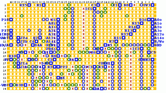 , component values
 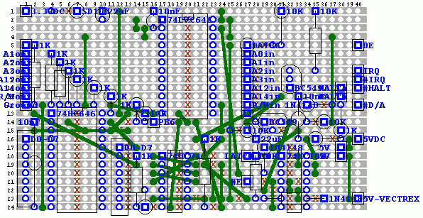 , VeroDes format ) was designed for building the initial prototype, and an alternative schematic using only components available in through-hole packages was created for breadboard prototyping (not tested, missing IRQ LATCH feature).
Initial testing was done using the 8-bit mode and a PC parallel port. For this a pitrexio-lpt library was used, and this will be provided here too when the latest version has been dug up. This could permit using the PiTrex with any PC that has a PCI parallel port card, though some issues with using the 8-bit mode were found during that testing.
PiTrex Discrete V. 2
While not yet begun, suggestions for a new version of the PiTrex have been made. The intention with these is not to significantly change the basic method of operation, so that compatibility with the first version should be maintained with relative ease, but to add more features on top of the core I/O functions.
The following ideas are being considered:
- If it becomes popular to develop for the Bare-Metal environment, then there really needs to be a serial port header on the PiTrex PCB, because that's the only way to access the Bare-Metal debugging interface.
- The DC socket is mainly of advantage to developers. Provision for it may be removed to free up space for new features and associated connectors.
- There is a 74LVC16646 IC which is basically two 74LVC646 ICs stuck together. In theory this would be much cheaper and use less board area than having two 74LVC646s. However the 74LVC16646 is only available in small SSOP/TSSOP packages, and in the past these have proved slightly beyond the limits of OmberTech's bulk PCB assembly abilities :). However it may be worth attempting.
- The IRQ Latch feature didn't work. Removal of this means that a single "1G" type AND gate package can be used for IC4, saving a lot of room. Though instead of dropping the feature, a programmable timer could be used that does the delay instead of the Pi0 at the end of a draw operation, therefore eliminating the need for strict timing in the software (the need to disable Linux system interrupts). Increasing the software performance might then also be easier. Should really look into the feasibility of using things like the Linux kernel high-resolution timer system before doing this.
- The Pi0 can not output sampled audio in Bare-Metal except through the Vectrex and its limited audio capacity. This is particularly an issue for reproduction of sounds from emulated arcade games, which generally used different and often more capable sound hardware. A basic solution is to use PWM output as in other Pi models, implementing the same circuit on the PiTrex and re-arranging the GPIO pins as described above. Though here there may also be quality issues with that approach, so it has also been suggested to add an Audio DAC to the board. As Bluetooth audio seems to work well with the Pi0w in Linux, and future emulator development is focused on Linux, it doesn't look like adding onboard audio support would be worthwhile at this stage. USB audio adapters can also be used in Linux if USB port access is possible by using alternative Pi0 orientations or an FFC USB cable.
- Connection to the PB6 signal from the Vectrex was a very poor solution for allowing communication between the Pi0 and a running Vectrex CPU. In practice it only permits communication from the Pi0 to the Vectrex if the Pi0 software knows the exact state of the A0-A3,A12,A14,A15 address outputs from the CPU at that time, and so also the exact time that the Vectrex would read the data (only possible by cycle counting). It may therefore be almost practically useless. True bi-directional communication on PB6 could be added, though there is some question as to the usefulness of this. Any co-processor type interations would still be sevierely limited by the speed of the serial communication over PB6. If it's used as a debugging system for development of regular Vectrex games, then the VecX emulator adapted to display via the Vectrex may be a more flexible option anyway.
- Software control of the HALT signal, instead of the current hardware jumper, would be required to permit switching between direct access of the VIA chip from the Pi0 (Vectrex CPU disabled), and communication with the Vectrex CPU (Pi0 VIA access disabled). So we'd probably want this if going with the above option.
- SRAM could be added, with suitable logic level conversion, so that the PiTrex could be used as a regular multicart as well. Again this means that the Vectrex CPU would be running, and therefore direct VIA access from the Pi0 would be impossible. However some of the associated circuitry might still be usable for logic level conversion. Again the VecX emulator is an alternative approach to this, which works with the existing hardware, and offers the potential for supporting USB/Bluetooth controllers as well.
- Alternative Pi orientation to allow access to USB and HDMI connectors. Requires current limiting to prevent overloading the Vectrex power supply, and larger filter capacitors to prevent glitches when USB devices are attached. Include mounting holes and hardware for attaching the Pi board securely, this requires longer than normal cartridge length and therefore limits the options for making cases.
The latter ideas are not really relevant to the original intent of the PiTrex project to access the Vectrex display from a Raspberry Pi Zero. They might be better suited to a more expensive "PiTrex+" model, attractive to people who don't already have a Vectrex multicart.
Further exploration of these ideas may be documented on a separate page later.