Hardware_Description
- Edit
- Recent Changes
- Advanced Search
- All Pages
- Administration
- Index
Hardware_Description 
The aim of the PiTrex is to allow a Raspberry Pi Zero
 (Pi0) to perform reads and writes from/to the 6522A VIA chip inside the Vectrex. The Pi0 features a General Purpose Input/Output (GPIO) header which can be used for the data exchange, but operates on 3.3V CMOS logic levels instead of the 5V TTL levels used inside the Vectrex. Further complicating matters is that for versatility and ease of running complex software such as emulators, the Pi0 should be expected to be running an Operating System such as Linux that (in common implementations) prevents real-time execution of software. This means that any software process may be delayed for an unknown time at the discretion of the OS, potentially missing the correct time for reading or writing data as required by the VIA which performs these operations according to the state of the Vectrex's internal "E" clock signal.
The function of the Vectrex's 68A09 CPU during operation is expected to be inhibited by taking the "#HALT" signal, exposed at the cartridge port, Low. Use of the Vectrex RAM and ROM ICs is not expected to be required by the Pi0, although these share the same bus as the VIA and may therefore be accessed by the same technique (but would require a new circuit board since this design does not support enough address lines to be able to access all of memory).
To work as a successful and reliable interface, the following functions therefore need to be performed by the PiTrex cartridge:
- Voltage level conversion of the Address bus signals, and bidirectional voltage level conversion of the Data bus signals, between 3.3V CMOS and 5V TTL
- Syncronisation of the Read and Write operations performed by the Pi0, with the 1.5MHz "E" clock signal used internally by the Vectrex (exposed in inverted form as "#E" at the cartridge port)
Vectrex Internals
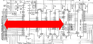
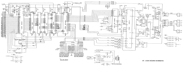
The digital component of the Vectrex circuitry is relatively straightforward. A common Data and Address bus is shared by the CPU with the cartridge port as well as all of the RAM, ROM, and, of importance to this project, the 6522A VIA chip. The VIA then controls the Digital-to-Analogue and Analogue-to-Digital conversion circuitry for the display and controller joysticks. It also accesses the AY3-8912 chip that generates sound and reads the digital controller inputs.
Address decoding for the RAM, ROM, and VIA is performed by a small network of NAND and OR gates (IC202 (74LS00) and IC203 (74LS32)). The VIA is selected if A12, A14 and A15 are High while A13 and A11 are Low. Bus conflicts are possible for some invalid Address states.
Control of the bus via the cartridge port is possible by pulling Low the #HALT input to the CPU, which is exposed on the cartridge port and normally pulled High by a 3K3 resistor. This disables the CPU, preventing it from executing instructions and making it place its Address and Data outputs in a High-Impedance state. The bus is then able to controlled via the cartridge port, and in this case by the Pi0. The 1.5MHz E clock output from the CPU remains active and is used by other ICs including the VIA.
Alternative methods of bus sharing with the 68A09 CPU are unable to be used because its the MRDY input is tied permanently High, so there is limited potential for a multi-processor type approach. The Pi0 is generally expected to replace the Vectrex CPU while the PiTrex cartridge is inserted.
The VIA is designed to trigger CPU Interrupts under certain conditions, and these are required for optimal handling of some common vector drawing processes (timer overflow interrupts). The Interrupt Request (#IRQ) output from the VIA is exposed on the cartridge connector, and may be used as an input to the Pi0 after logic level conversion, or used by the PiTrex hardware to trigger a prepared read or write operation immediately (without waiting for the Pi0 to respond).
PiTrex Hardware Designs
Two concepts for the PiTrex hardware have been proposed:
- Discrete logic design based on two 74LVC646 bidirectional bus buffers with 3V3 CMOS to 5V TTL level conversion capability. Address and Data signals transfered to/from the Pi0 in parallel over GPIO.
- Programmable logic design based on a Programmable Logic IC with 5V TTL compatible I/O. Address and Data signals transfered to/from the Pi0 serially using SPI protocol over GPIO.
Currently the discrete logic design is working and supported in the current codebase. The programmable logic based design is still under development by James Churchill.
Discrete Logic PiTrex
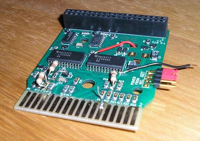
PiTrex cartridges to this design will be available from OmberTech
 soon.
soon.Overview
This design, developed by Kevin Koster, latches the Address and/or Data bus state for a read or write operation after the LATCH EN output from the Pi0 goes High. In sync with the falling edge of the E signal on which the VIA samples the Address and Data bus, it reads/writes the provided signals from/to the Vectrex bus. A Ready (RDY) output signals to the Pi0 when the operation is complete an a new read or write may be performed.
Alternatively, the same procedure can be performed by driving the IRQ LATCH input High to signal a read or write, while LATCH EN remains Low. This prevents the operation from being performed until the #IRQ output from the VIA is asserted. This allows immediate resposes to expected interrupts to be performed, such as disabling the vector beam immediately as a timer overflow interrupt indicates the end of a line being drawn.
A jumper may be fitted, which is inserted to pull the #HALT input to the CPU Low. This allows the PiTrex cartridge to be connected while the Vectrex CPU is operating, but the #HALT input to the Pi0 must be checked by the PiTrex software to ensure that this jumper is inserted, and the CPU is therefore not using the Vectrex bus, before allowing any read or write operations to be performed.
Two 74LVC646 bidirectional latching bus buffer ICs are used. One provides for the eight bit data bus, while the other controls the minimal number of Address lines required for addressing the VIA. The VIA requires only four Address lines (A0-A3) for selecting its internal registers, and three others (A12, A14, A15) are required to select the VIA via the Address decoding circuitry in the Vectrex. Other address lines are permanently tied Low to disable the RAM and ROM ICs. The R/#W ouput is also passed through in sync with the Address bits, as well as a signal to the PB6 I/O line of the VIA directly.
Power
The power required by this PiTrex design itself is minimal (measured under 2mA), but the Pi0 may draw over 200mA at 5V during use. Mixed success has been observed using the 5V supply from the Vectrex to provide this power, so facility is provided for optionally powering the Pi0 and the PiTrex cartridge from an external 5V supply such as USB. A jumper is provided that may be fitted to enable drawing power from the Vectrex, otherwise a centre-positive DC socket on the PiTrex cartridge, or a micro USB connector on the Pi0, may be used to connect an external 5V supply. If an external power supply is used, the "POWER FROM VEC." jumper _must_ be removed.
Due to the unknown effects of additional power dissipation from the 5V voltage regulator inside the Vectrex when it supplies power to the Pi0, use of an external power supply is recommended even were powering from the Vectrex is successful.
Power consumption of devices connected to the Pi0 via USB or HDMI should also be considered.
Measurements of power consumption of Raspberry Pi Zero 
Reading and Writing
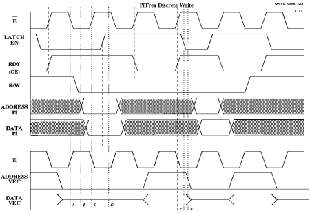
The sequences for reading and writing from to/from the Vectrex using this PiTrex design is performed by the software running on the Pi0 folling these steps:
Write
  A *Pi sets LATCH EN Low.
  B *Pi sets R/W' output Low.
  C *Pi sets other Address outputs, and Data outputs.
  D *Pi sets LATCH EN High (address and data is latched by buffer ICs IC1 and IC2).
  E *Data has been written after OE' input goes Low to High (and will be again until interface is disabled).
  F *Pi sets LATCH EN Low to disable interface.
Read
  A *Pi sets LATCH EN Low.
  B *Pi sets Data I/O lines to input mode.
  C *Pi sets R/W' output High.
  D *Pi sets other Address outputs.
  E *When OE' High, Pi sets LATCH EN High (address and data is latched by buffer ICs IC1 and IC2).
  F *Data is valid after OE' input goes Low to High (and after that until interface is disabled).
   Pi reads Data.
  G *Pi sets LATCH EN Low to disable interface.
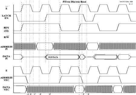
At a hardware level, these diagrams describe the signals on the Pi0 side, and on the Vectrex side, of the PiTrex cartridge (stages described above are marked by letters at the bottom of the diagrams):
These diagrams are also available in PDF format
 .
.Functions for performing reads and writes with the VIA are provided in pitrexio-gpio.c as part of the PiTrex software codebase.
8-Bit Mode
Basic hardware support is implemented for using this PiTrex design with computers other than the Pi0 which have only an 8-bit parallel data bus available. In this mode the #D/A input, connected to a Raspberry Pi GPIO pin that is tied permanently to GND when it is inserted, is toggled to alternately load the Data and Address bytes into the bus buffers before the Read or Write operation takes place.
Besides the 8-Bit parallel bus which connects in parallel to both the Address and Data lines normally running to the Pi- GPIO, separate lines to control #D/A and LATCH EN are required, as well as an input to read RDY. IRQ LATCH may also be used.
The jumper J3 may need to be made to enable correct operation in this mode, formed as a solder bridge on the bottom of the circuit board (under D4).
Initial testing of writes using a PC Parallel Port were performed with this mode using the functions in pitrexio-lpt.c, which has not been tested extensively since. Other platforms where the 8-Bit mode may be useful are vintage computers such as the Commodore 64 with its User Port (which is also controlled by a 6522 VIA chip, as it happens). Due to the asynchronous access enabled by the PiTrex hardware, there is no need for the clock speed of the controlling computer to be equal or greater than the 1.5MHz clock used by the 6522.
Technical Details
See the PiTrex_Discrete page for a full circuit description and more technical notes on the electronic design.
Programmable Logic PiTrex
This design
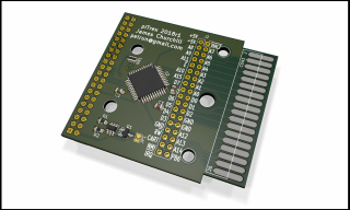
 , in development by James Churchill, passes Address and Data states serially to a Programmable Logic IC which reads/writes the Vectrex bus using its 5V tolerant I/O pins, in sync with the Vectrex's E clock signal. With this design, the full 16bit Address bus can be controlled, allowing the ROM and RAM ICs to be accessed as well as the VIA. The hardware SPI support of the Pi0 chipset can be used to perform the serial data exchange with the PiTrex using its GPIO.
Currently an initial schematic and circuit board design have been developed. The code for the Programmable Logic IC is still under development and the exact process for reading/writing to the VIA has not been documented. There is no suport for this design in the current PiTrex codebase.
Raspberry Pi and Other Computer Hardware
Single-Board Computers
The PiTrex is primarily targeted at the Raspberry Pi Zero  and Raspberry Pi Zero W
  .
.
These feature the following key specifications:
- 1GHz single-core ARM V6 CPU
- 512MB DDR2 RAM
- 40pin GPIO Header with 28 configurable Input/Output pins. Built-in hardware UART, SPI, I2C, PWM, etc. Programmable Pull-up/Pull-Down/High-z state on any input. Connections to 5V input, and 3V3 output from onboard voltage regulator. Notes
 . Unpopulated, except on Raspberry Pi Zero WH
 - 1x Micro USB 2.0 Port
- 1x MicroSD Card slot (SDHC compatible)
- 1x Mini HDMI Port
- 1x Composite video output (2pin header) Unpopulated
- Hardware Reset Signal Input
- CSI camera connector
- 802.11 b/g/n wireless LAN Raspberry Pi Zero W only
- Bluetooth 4.1 Raspberry Pi Zero W only
- Bluetooth Low Energy (BLE) Raspberry Pi Zero W only
The Raspberry Pi Zero is designed around the BCM2835  SoC IC (Datasheet
  ), as used at a lower clock speed in the original Raspbery Pi 1, and from which SoC ICs used for other Raspberry Pi boards are derrived.
The Raspberry Pi 2 and later models share a compatible GPIO header, while featuring more powerful CPU and larger RAM options. In particular, models offering multi-core CPUs may allow for a significant performance advantage to be gained by using one core to run a process monitoring the status of Read/Write operations as indicated by the RDY signal from the PiTrex (Discrere). Note that although the GPIO pinout is the same, the changes in the SoC should be analysed to ensure that the current pitrexio-gpio code is compatible.
A further, rather obvious disadvantage to using other Raspberry Pi boards is that they are unlikely to fit within a practical cartridge form-factor. Connection to the GPIO header using a ribbon cable is possible, though care should be taken to ensure the correct pin-out (IDE Hard Disk cables will not work unless the cable or one of the GPIO header connectors is modified).
A large variety of Raspberry Pi clones have been developed by Chinese companies. In addition to the form factor issues, these often feature different SoC ICs which in turn require significant change to the existing pitrexio-gpio code in order to be used, and may have different GPIO pinouts. However one model of the Open-Source "Banana Pi" designs follows the same form-factor as the Raspberry Pi Zero, as well as featuring a compatible GPIO header. The Banana Pi Zero  offers a quad-core CPU and faster RAM, so it could be a significant performance improvement over the Raspberry Pi model. It does use a different SoC of course, so a different version of the GPIO code will have to be written to suit it, though there appears to be a modified version of the BCM2835 library
  to work with it, which might make the task relatively easy (though on second thoughts, that library may not be compatible with the Allwinner H2+).
Key Specifications:
- 1.2GHz quad-core ARMv7-A CPU (some sources say 1GHz, though the Allwinner H2+ is rated up to 1.296GHz)
- 512MB DDR3 RAM
- 40pin GPIO header hardware compatible with Raspberry Pi (allegedly, but checked it will work with the PiTrex Discrete)
- 1x Micro USB 2.0 port
- 1x MicroSD card slot (SDHC compatible)
- 1x Mini HDMI Port
- Onboard Power and Reset buttons
- CSI camera connector
- 802.11 b/g/n wireless LAN (optional 802.11ac (AP6335))
- Bluetooth 4.0 (optionally without Bluetooth, but lower power consumption (AP6181))
- 3pin Debugging UART
Note: No Composite video output.
The Banana Pi M2 Zero uses the [https://linux-sunxi.org/H3|Allwinner H2+] SoC, which is almost the same as the Allwinner H3  . Allwinner H3 Datasheet
  .
.
A good review and comparison  .
.
GPIO
Other Banana Pi models use different SoCs, so things like the modified BCM2835 lib that target other boards won't work. Focus on the SoC, which actually means the Allwinner H3 because the H2+ us just a variant of that.
There's a version of the Wiring Pi  library that has been modified to support all of the Banana Pi boards including the M2 Zero. But it's probably easier to study this library
  which targets just the Allwinner H3.
It's would be easiest to just replace the few BCM2835 library functions that we use with modified versions based on the register addresses etc. used by that H3 GPIO library. Though that lib. itself works quite differently.
Other Computers
While primarily targeted at small single-board computers which can be connected conveniently to the PiTrex cartridge, connection to PCs or vintage computers is not excluded from possibility. The PiTrex Discrete design includes an 8-Bit mode, described above, which permits using computers with more limited parallel I/O than the Raspberry Pi Zero. Initial testing has been done with a PC via the Parallel Port.


